News
What Are the Challenges in Designing PCBs for Automated Test Equipment (ATE)?
In the development and production of printed circuit boards (PCBs), there are critical stages that require precise and automated testing to ensure the final product meets the required standards. Automated Test Equipment (ATE) plays a central role in ensuring the quality of PCBs, especially in large-scale manufacturing processes. Designing PCB that can be tested using ATE involves unique challenges that designers must address to ensure the tests are effective, accurate, and efficient.
In this article, we will explore the key challenges in designing PCBs for Automated Test Equipment (ATE) and how to address these challenges during the design and production process.
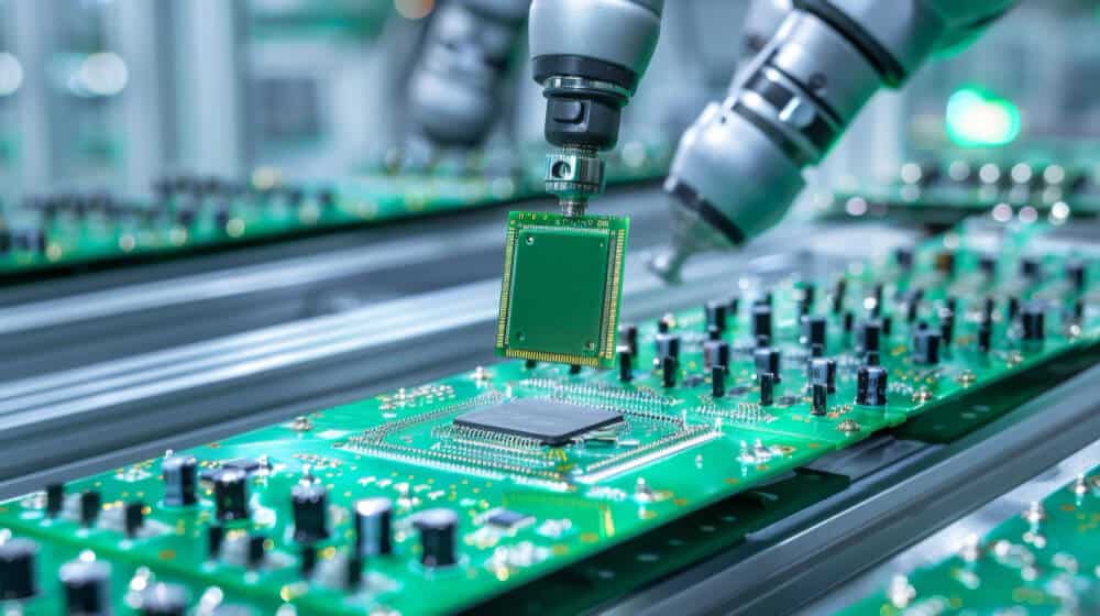
Physical Access to Components
One of the initial challenges in designing PCBs for ATE is ensuring physical access to the various components on the board. When automated equipment tests a PCB, direct access to test points on the board is required to measure electrical signals and perform functional tests.
- Component Density: The higher the component density on the board, the more difficult it becomes to ensure access to all required test points. This complicates connecting the test points to the ATE equipment and increases the risk of incomplete or inaccurate testing.
- Well-Defined Test Points: Test points must be strategically placed to be accessible to the mechanical probes or arms of the automated testing system.
Compatibility with Advanced Testing Equipment
Automated testing requires the PCB to be compatible with the testing equipment being used. Tools such as In-Circuit Testing (ICT) or Flying Probe Testing demand that the PCB design meets the mechanical and electrical requirements of the equipment.
- ICT Compatibility: This type of testing requires clear and accessible test points, as well as board dimensions that fit the testing apparatus. The PCB design must facilitate the testing of current and voltage at the required points.
- Flying Probe Design Considerations: In cases where Flying Probe Testing is used, the PCB structure must allow efficient testing of the components, ensuring easy access to each component on the board.
Signal Communication and Power Supply
During the PCB design process for ATE, the signal communication and the ability to supply power to various components during testing must be carefully considered.
- Component Functionality Testing: To test the proper functioning of each component, the design must ensure that adequate power is supplied to every part of the board. Improper design may result in the inability to supply the necessary voltage during testing, making it difficult to identify faults.
- Noise Filtering: Testing must be conducted in an environment free of electrical interference. Proper PCB design, including filtering and shielding from noise, is essential to prevent external influences from affecting test results.
Electrical Signals and Routing Path
Proper design of the electrical signal paths on the board is a critical factor when designing a PCB for automated testing.
- Cross-Talk Prevention: A well-designed PCB isolates different signal paths to prevent cross-talk, which could interfere with the accuracy of the tests and lead to false failures. Signal lines that are too close can lead to signal disruption, reducing the reliability of the tests.
- Routing Directions: Proper signal routing ensures continuous data flow and power supply, allowing the ATE system to perform the required tests with minimal external interference.
Environmental Stress Testing
In cases where the PCB is required to operate in harsh environmental conditions (such as high temperatures, humidity, or exposure to chemicals), the environmental conditions during the testing process must also be considered. Proper PCB design and material selection must withstand these conditions to ensure reliable testing.
- Durable Materials: Materials that are resistant to the conditions in which the tests will be conducted must be selected. For instance, heat and moisture-resistant materials improve the accuracy of test results and prevent future failures.
- Temperature and Humidity Testing: The PCB must be designed to undergo testing in high-temperature and high-humidity conditions, especially for systems intended to operate in extreme environments.
Compliance with Testing Standards and Regulations
During the PCB design process for ATE, it is essential to ensure that the design complies with industry standards and regulations relevant to the field in which the PCB will be used.
- Compliance with International Standards: The PCB must be designed according to industry-recognized standards such as IPC, MIL-STD, and other relevant customer requirements.
- Quality Control: ATE is used to ensure comprehensive quality control of the board, so each stage of the design process must align with the testing requirements to demonstrate durability and reliability under the conditions in which the PCB will be tested.
Conclusion
Designing PCBs for Automated Test Equipment (ATE) is a complex process that requires consideration of a wide range of technical and mechanical factors. From physical access to components and ensuring compatibility with advanced testing equipment to environmental stress resistance and compliance with testing standards, each of these considerations significantly affects the ability of the PCB to pass automated tests accurately and efficiently. Proper design ensures that the produced boards meet the highest standards of quality and reliability.
More News Articles