News
Introduction to ESD – Electrostatic Discharge
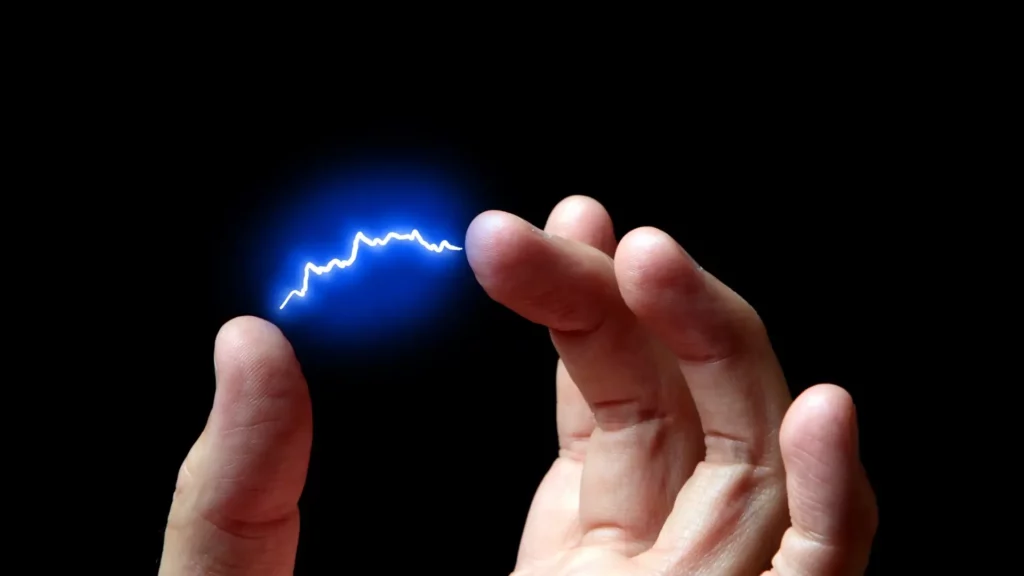
You may sometimes feel an electric shock when you touch another object. For example, when walking down a hotel corridor, you may get a small shock when you press the elevator button. These shocks, harmless to ourselves, are caused by a build-up of a static electric charge on our bodies that can reach several thousands of volts. The shock we feel is caused by the static rapidly discharging into another object—often the earth.
ESD is normally harmless to us because it is a very fast phenomenon – lasting much less than a millionth of a second – and therefore has a relatively low amount of total energy compared to the size of our bodies. Modern semiconductor devices, in contrast, have ever decreasing geometries and can be very sensitive to even the smallest of ESD events (including events too small for us to feel). This raises a major reliability concern for semiconductor designers which they invariably address by embedding protection structures into their integrated circuits.
The whole subject of semiconductor reliability is very broad, but it is clear that each design must be subjected to a range of tests to ensure that it can meet the robustness and life expectancy demands of its application in the real world. Generally known as qualification testing, checking the correct operation of the ESD protection structures is part of this activity. There are several models which are commonly used to qualify semiconductor devices for susceptibility to ESD:
Human Body Model (HBM)
the so-called Machine Model (MM)
Charged Device Model (CDM)
The HBM and MM are broadly similar, in that a capacitor is charged to a known potential and then discharged into the device under test (DUT) via a known impedance. The HBM uses 100pF discharged through 1,500 ohms and the MM uses 200pF discharged through nominally zero ohms although in practice the impedance must approximate to 10 ohms in series with 0.75uH.
The HBM stems from the US Mil-Std 883 test method 3015.x and the MM originated from Japan’s EIAJ testing standards. It has been said that the Machine Model is actually mis-named and that it is really the Japanese human body model rather than an attempt to model a discharge coming from a charged machine as opposed to a charged human. In reality the history and origins of the test methods does not matter. The standard models simply allow a way to test and compare the ESD robustness of a device in a well-understood and repeatable way.
There has always been much debate about the relative attributes of HBM and MM testing but there is substantial evidence that both are essentially testing the same failure mechanism within an IC. For the same charge voltage HBM testing results in much lower currents than MM (because of the higher series impedance) so a device’s HBM failure threshold is often an order of magnitude greater than it’s MM failure threshold. As mentioned above, this does not matter as long as a like-for-like comparison can be made. Many IC users are satisfied with an ESD classification of 1kV HBM or 100V MM, although modern high performance ICs often struggle to achieve these levels without a detrimental effect on their performance.
Commercial HBM and MM test systems have a fixture which can hold the DUT in an IC socket and connect each pin to the HBM or MM discharge network using some form of switching mechanism which can be based on mechanics, relays or a combination of the two.
Whereas HBM and MM address external objects discharging into the IC, CDM is based on the IC itself becoming charged and then discharging to earth. As mentioned earlier, ICs are very small relative to most external objects and this has an impact on the speed of the ESD event. HBM and MM events last for times of the order of 100ns with a rise time normally in the range 2ns to 10ns. CDM events are much faster than this, typically lasting less than one nanosecond with rise times of the order of 100ps (100 trillionths of a second). As might be expected, the type of damage caused by CDM is characteristically different to HBM and MM and the protection techniques deployed by the IC designer are also different.
It isn’t feasible to generate proper CDM events when a device is in a socket because the physical characteristics of the socket would overwhelm those of the IC package. Commercial CDM test systems have a fixture which can hold the bare DUT on a ground plane. The DUT is charged up, either directly via a probe or indirectly by induced field before being discharged by another probe.
Electrostatic Discharge (ESD): An Invisible Threat to Electronics
Electrostatic discharge (ESD) refers to the sudden movement of electrical current between two objects with differing electrical charges. In electronics, ESD is a serious issue as it can harm or even destroy delicate components. This happens due to the quick burst of current that creates electrical fields that can interfere with a device’s internal circuitry. Imagine rubbing a balloon on your hair and then sticking it to a wall, that’s a simple example of static electricity in action. When the balloon touches the wall, a small discharge occurs, causing it to stick. Similarly, in electronics, discharges between components can lead to damage.
Protecting Electronics from ESD Damage
Manufacturers use several techniques to guard electronics against ESD. One method involves building protection into the devices themselves. This can mean using ESD resistant materials, adding protective layers, or integrating circuits that can absorb or deflect ESD currents. Another way is through external protections like ESD safe packaging, which stops static charge from building up during shipping or storage. Additionally, strict handling protocols are followed to lower the risk of ESD, such as wearing ESD safe gloves and using grounded workstations to release static electricity.
Why ESD Testing is Crucial for Electronics
To make sure their products are protected against ESD, manufacturers carry out thorough testing. Standard ESD tests include the Human Body Model (HBM), Machine Model (MM), and Charged Device Model (CDM). Each test simulates different ESD scenarios to see how vulnerable a device is to damage. The HBM test mimics a discharge from the human body, the MM test simulates one from a machine, and the CDM test assesses the risk of damage when a charged device contacts a neutral surface. These tests help manufacturers detect weak points and improve ESD protection in their designs.
Managing Static Electricity: Key to ESD Safety
Electrostatic dissipation is the controlled release of static electricity to stop charge buildup. This is done by using materials that conduct electricity well, allowing static charges to safely dissipate and lowering the risk of ESD. In electronics manufacturing, this includes using ESD safe work surfaces, wrist straps, and grounding mats. Incorporating these techniques helps create a safer environment for handling delicate electronics.
More News Articles