News

Boston Semi Equipment’s Odyssey Takes the EG2001 Wafer Probe Platform into the Future

BILLERICA, Mass. – July 14, 2015 – Boston Semi Equipment (BSE) today announced its new Odyssey model wafer prober for 2-inch to 8-inch and custom geometry wafers. The Odyssey takes the proven mechanisms of the EG2001, supports them with enhanced software and electronics, and delivers a fully EG2001 compatible platform that is able to accommodate present and future probe requirements.

“The Odyssey is a high throughput, pc-based platform with 3 micron accuracy,” commented Colin Scholefield, Boston Semi Equipment Executive Vice President. “With features that include a touchscreen interface, integrated wafer mapping software and PROMS that permanently store profiling data; the Odyssey is a cost effective choice for high performance, reliable and flexible wafer probe applications.”

The Odyssey is designed to be fully compatible with the EG2001 making it easy to integrate into existing EG2001 environments. The pc-based control system ensures the platform can be enhanced to satisfy market requirements now and into the future and the Odyssey’s modular architecture easily adapts and expands to changing requirements. Boston Semi Equipment’s probe engineering team is available to develop custom solutions for specific customer requirements.

All Boston Semi Equipment wafer probe solutions are supported by experienced service technicians who are providing industry leading support every day.

About Boston Semi Equipment

Boston Semi Equipment LLC (BSE) provides equipment and services to semiconductor manufacturers and OSATs worldwide. Our solutions address customer requirements for testing, handling, inspecting and manufacturing semiconductors. BSE helps customers maintain maximum uptime by providing a broad range of service and support products. Our goal is to lower equipment costs for our customers. Visit www.bostonsemiequipment.com for more information.

Company Contact
Colin Scholefield
Boston Semi Equipment
[email protected]
Tel: +1 781 273 0090

Media Contact
Amy Smith
Impress Labs
[email protected]
Tel: +1 401 369 9266

More News Articles

הדפסת תלת מימד

Admati to Host its 3rd Biannual Semiconductor Seminar

The semiconductor industry is getting excited as Admati Agencies is getting ready to host its 3rd biannual Admati Semiconductor Seminar, on April 10th, at the Hilton Tel-Aviv. In the past 5 years Admati’s seminar became the place where semi’s professionals from leading companies meet and learn about the latest developments in the fields of backhand validation, and device test and…

Thank You Everyone

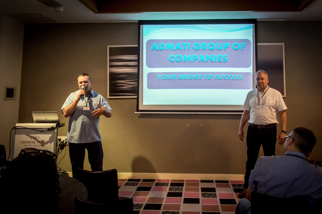
We wanted to say a quick thank you to everyone who came and visited our Admati Seminar at the Crown Plaze City Center in TLV. Thanks to you we had another great seminar with many attendees and great experience. We are sure you all had a great time and made some new connections. Here are some great photos from the…

עיבוד שבבי CNC

What Are the Advantages of CNC Machining Compared to Conventional Machining?

CNC (Computer Numerical Control) machining has become one of the most prevalent technologies in modern manufacturing. While conventional machining has been used for decades, CNC offers numerous advantages in terms of precision, efficiency, and flexibility. In this article, we will examine the key benefits of CNC machining compared to traditional methods and explain how this technology revolutionizes manufacturing across various…

What is the difference between laser cutting, laser engraving, and laser micro-machining?

Does your project require laser material processing? It is very important to distinguish between laser cutting, laser engraving, and laser micro-machining. You can save time, money, and problems if you know how and when it is right to apply each method. Laser cutting – precision and speed in a clean and efficient process Focused laser cutting locally heats the material…

Open chat
Hello 👋
Can we help you?