חדשות

Admati to Host its 4th Biannual Semiconductor Seminar

Once again Admati is hosting its bi-annual Semiconductor Technical Seminar. As in years past, the seminar will take place in the Tel-Aviv Hilton, and will be an opportunity for Semi’s professional to meet again. The seminar will take place in April 28th,and will start at 8:30 and end at 17:00. Mr. Admati, Admati’s Chairman and Owner, said “as always the company sees the seminar as an opportunity for our old and new friends to meet and discuss new ideas and developments of the industry”.


The Seminar will include the following topics, ID’s WLCSP Probe head solutions, Microseries and Monet, Thermal Management during Burn-In and Test, BiTS interconnect for next generation devices, Nano-Surgery and Analysis, Board Level Reliability Testing, and JS001-2014 HBM ESD testing standard. In addition the seminar will host, as guest speaker, Prof. Avishai Braverman, former president of the Ben-Gurion University of the Negev, served as a member of the Knesset for the Labor Party between 2006-2015, and as Minister of Minorities affairs between 2009-2011. He received his PhD in economics from Stanford University. Mr. Broverman, also, served for fourteen years as a senior official in the World Bank in Washington.

As in the past, the registration to the seminar is free, and includes full hospitality and free parking at the Hilton’s parking lot. Please note that the preregistration is required. You can register here.

Looking forward to seeing you there!

מאמרים נוספים

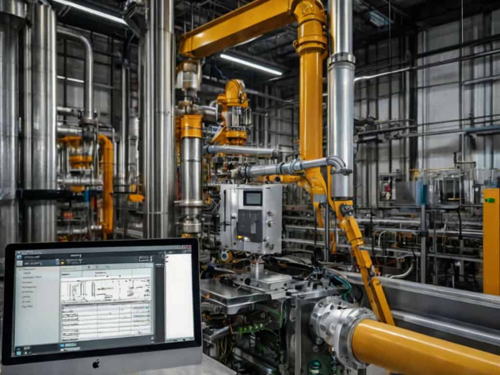
שגיאות נפוצות בתהליך עיבוד שבבי וכיצד להימנע מהן

תהליך עיבוד שבבי משמש לייצור רכיבים מדויקים עבור תעשיות כמו רפואה, תעופה ואלקטרוניקה. סטייה קטנה באחד משלבי העבודה עלולה לגרום לפסילת חלקים, לעכב את לוחות הזמנים ולהגדיל את עלויות הייצור. לכן, היכרות עם הטעויות הנפוצות ועם הדרכים למנוע אותן מראש היא תנאי לייצור מדויק, עקבי ואמין. מדוע טעויות בתהליך עיבוד שבבי עלולות להיות יקרות? תהליך עיבוד שבבי דורש דיוק גבוה…

הדפסות במתכת

הדפסות במתכת

הדפסה במתכת היא אחת הטכנולוגיות המתקדמות בייצור מדויק, המאפשרת לייצר חלקים מורכבים ישירות מקובץ דיגיטלי. בתעשיות מתקדמות כמו תעופה, ביטחון ורפואה מיישמים הדפסה במתכת לייצור רכיבים שלא ניתן לייצר בשיטות מסורתיות. מהי הדפסה במתכת? הדפסה במתכת (Metal Additive Manufacturing) היא שיטה תעשייתית מתקדמת לייצור חלקים מאבקת מתכת, שכבה אחרי שכבה. לעומת עיבוד שבבי, המתבצע על ידי הסרת שכבות חומר לעיצוב…

PCB מעגלים מודפסים

שימושים נפוצים של מעגלים מודפסים (PCB) בתעשייה

מעגלים מודפסים (PCB – Printed Circuit Boards) מהווים מרכיב מרכזי כמעט בכל מכשיר אלקטרוני מודרני. הם מספקים תשתית פיזית וחשמלית לחיבור רכיבים אלקטרוניים ומאפשרים זרימה של חשמל ושליטה מדויקת בפעולות מכניות ודיגיטליות.  ל-PCB ישנם שימושים שונים בתעשיות שונות – את העיקריות נציג כאן. אנחנו כאן כדי לעזור לכם להבין עד כמה רכיבים אלה נמצאים בלב התעשייה המודרנית. מהם מעגלים מודפסים?…

יציקות לחץ

יציקות לחץ

יציקות לחץ (Die Casting) משמשות לעיבוד מדויק של חלקים מתכתיים בתהליכי ייצור תעשייתי. יציקת לחץ מאפשרת לייצר חלקים בצורות מורכבות בנפחי ייצור גבוהים, תוך שמירה על סובלנות הנדסית הדוקה. מהי יציקת לחץ? יציקות לחץ הן תהליכי ייצור המבוססים על הזרקת מתכת נוזלית לתוך תבנית (Die) בלחץ גבוה. רמת הלחץ נשמרת גבוהה עד לקירור ומיצוק המתכת, ולאחר מכן החלק מוצא מהתבנית….